S. Swordy is the Group Coordinator for the camera/electronics task and, working with the VERITAS Project Manager, will oversee the project ensuring that the work stays on schedule and within budget, and that the interface requirements and other specifications of the FADC are met.
J. Buckley (Faculty, Washington University) working with Paul Dowkontt (electrical engineer, Washington University) will jointly complete the design of the electronics, and will oversee the FADC subproject. The Washington University electrical engineer will be responsible for the design and entry of the electronics schematics (for the FADC board, clock/trigger board, and J3 backplane), but will work with an outside consulting firm (Avid Technologies Inc) to do the printed circuit board (PCB) layout. Parts ordering, oversight of PCB manufacturing and layout, final electronic and mechanical assembly, and automated board testing will be the responsibility of an electronics technician, G. Simburger.
J. Buckley and a graduate student will design the elements of the data acquisition software required for designing the FADC data interface, and for designing the automated test setup.
The University of Chicago will take responsibility for the design of the FADC data acquisition computer and reflective memory which will merge the data from the three FADC crates, and will provide a high speed buffered interface to the data acquisition hardware. The University of Utah will build the CFD daughter boards or will work with CAEN to produce these. The University of Utah will also work on the thermal control system for the FADC electronics.
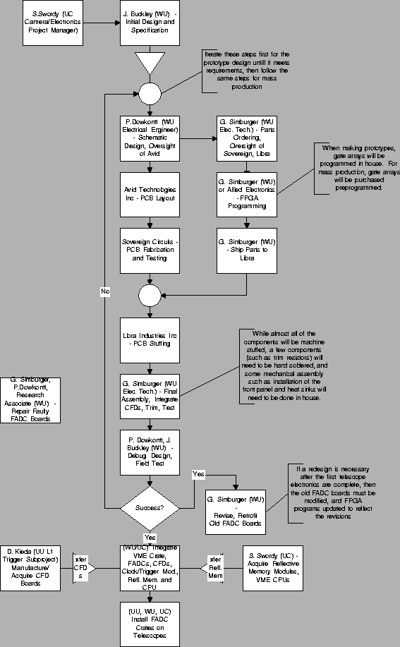
Figure 7 shows a flow chart of the FADC/CFD system design and fabrication.
The design starts with J. Buckley and is passed to P. Dowkontt who completes the detailed schematics. This design is passed on to Avid Technologies who complete the PCB layout working closely with P. Dowkontt. G. Simburger will oversee the remainder of the project. G. Simburger will order components for the boards, and initiate work at Sovereign Circuits who will fabricate and test PCBs. G. Simburger will send PCBs and Components to Libra Industries, who will machine stuff the boards. The completed boards will be returned to G. Simburger for final mechanical and electronic assembly and testing using an automated test station consisting of Wiener NIM and VME racks with a crate CPU. D. Kieda will supply CFD daughter cards, and S. Swordy will supply reflective memory modules, CPUs and Wiener Crates to be assembled at Washington University before shipping to Arizona.